Blog
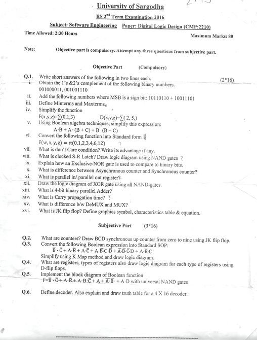
Digital Logic Design BSSE 2nd Term Past paper 2016 UOS

University of Sargodha
BS 2nd Term Examination 2016
Subject: Software Engineering
Paper: Digital Logic Design (CMP:2210)
Time Allowed: 2:30 Hours
Maximum Marks: 80
Objective Part (Compulsory) (2*16)
Q.1. Write short answers of the following in two lines each.
i. Obtain the 1’s & 2’s complement of the following binary numbers.
- 00100011, 00101100
ii. Add the following numbers where MSB is a sign bit:
- 10110110 + 10011011
iii. Define Minterms and Maxterms.
iv. Simplify the function
- F(x,y,z) = ∑(0,1,3)
- D(x,y,z) = Σ(2,5)
v. Using Boolean algebra techniques, simplify this expression:
- A + B + (B + C) + (B)
vi. Convert the following function into Standard form:
- F(w,x,y,z) = π(0,2,3,4,6,12)
vii. What is don’t care condition? Write its advantage if any.
viii. Explain an Exclusive-NOR gate and its use to compare binary bits.
ix. What is the difference between Asynchronous and Synchronous counter?
x. Draw the logical diagram of XOR gate using all NAND gates.
xi. What is a binary half adder?
xii. What is binary propagation time?
xiii. What is the difference between DeMUX and MUX?
xiv. What is JK flip flop? Define graphics symbol, characteristics table & equation.
Subjective Part (31*16)
Q.2. What are counters? Draw BCD synchronization up counter from zero to nine using JK flip flop.
- BCD = A + B + A’B + A’B’C + A’B’C’
- Simplify using K-map method and draw logic diagram.
Q.3. What are registers? Types of registers also draw logic diagram for each type of registers using:
- Registers with enable,
- D flip-flop,
- J-K flip-flop.
Q.4. Write the logic diagram of Boolean expression:
- F = B’C + A + B + A’B + A’D with universal NAND gates.
Q.5. Define decoder. Also explain and draw truth table for a 4 x 16 decoder.
