Blog
Digital Logic Design BSIT 2nd Term Past paper 2016 UOS

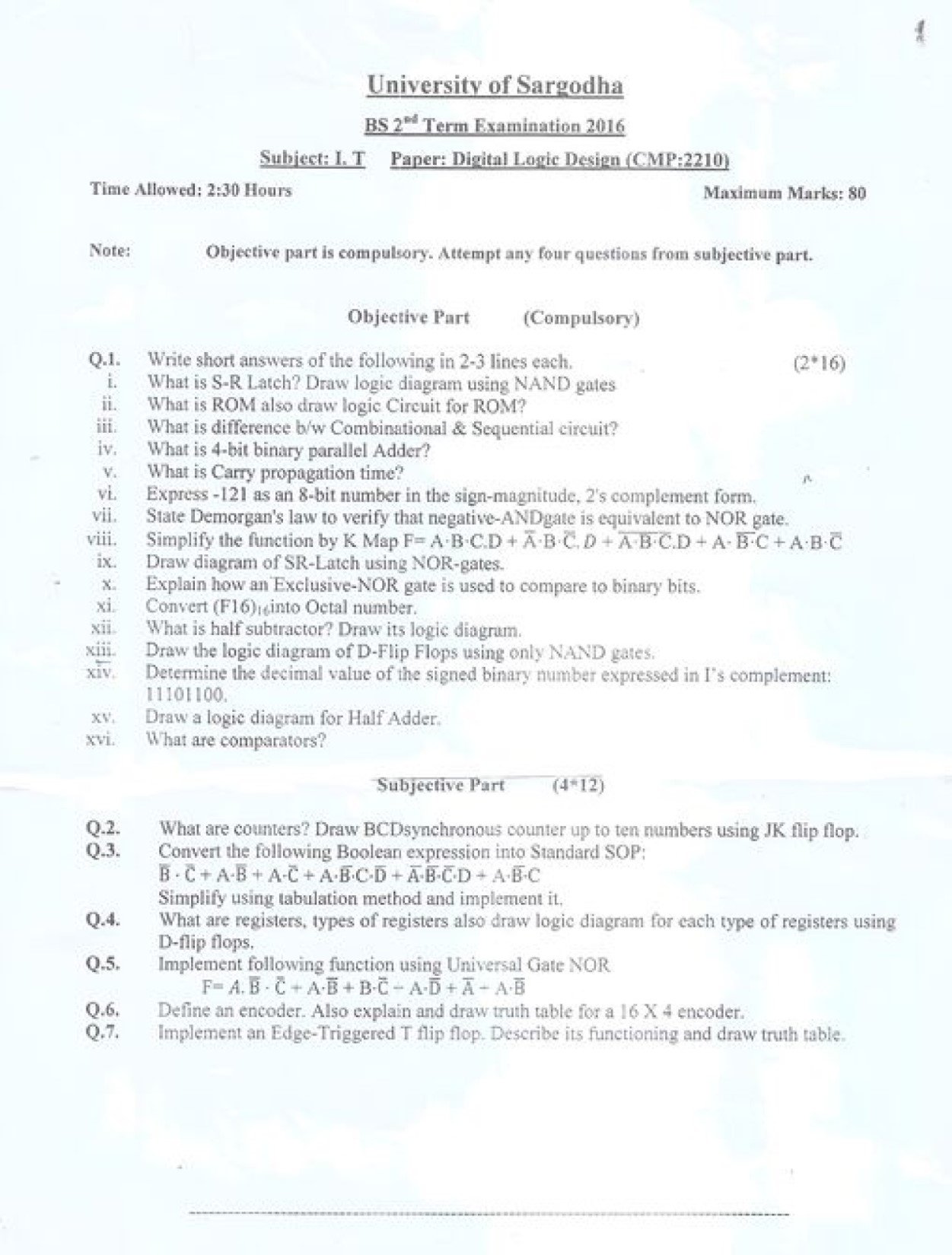
University of Sargodha
BS 2nd Term Examination 2016
Subject: I.T
Paper: Digital Logic Design (CMP:2210)
Time Allowed: 2:30 Hours
Maximum Marks: 80
Objective Part (Compulsory)
Q.1. Write short answers of the following in 2-3 lines each. (2*16)
i. What is S-R Latch? Draw logic diagram using NAND gates.
ii. What is ROM also draw logic Circuit for ROM?
iii. What is difference b/w Combinational & Sequential circuit?
iv. What is 4-bit binary parallel Adder?
v. What is Carry propagation time?
vi. Express -121 as an 8-bit number in the sign-magnitude, 2’s complement form.
vii. State Demorgan’s law to verify that negative-AND gate is equivalent to NOR gate.
viii. Simplify the function by K Map F = A·B·C·D + A·B·C·D + A·B·C + A·B·C·B.
ix. Draw diagram of SR-Latch using NOR gates.
x. Explain how an Exclusive-NOR gate is used to compare to binary bits.
xi. Convert (F16)16 into Octal number.
xii. What is half subtractor? Draw its logic diagram.
xiii. Draw the logic diagram of D-Flip Flops using only NAND gates.
xiv. Determine the decimal value of the signed binary number expressed in 1’s complement: 1101100.
xv. Draw a logic diagram for Half Adder.
xvi. What are comparators?
Subjective Part (4*12)
Q.2. What are counters? Draw BCD synchronous counter up to ten numbers using JK flip flop.
Q.3. Convert the following Boolean expression into Standard SOP:
B’·C + A·B’ + A·C + A·B·C’D + A·B·C + A·B.
Q.4. What are registers, types of registers also draw logic diagram for each type of registers using D-flip flops.
Q.5. Implement following function using Universal Gate NOR:
F = A·B ·C + A·B·B’ + C·B’ – A·D + A ·B.
Q.6. Define an encoder. Also explain and draw truth table for a 16 X 4 encoder.
Q.7. Implement an Edge-Triggered T flip flop. Describe its functioning and draw truth table.
