Blog
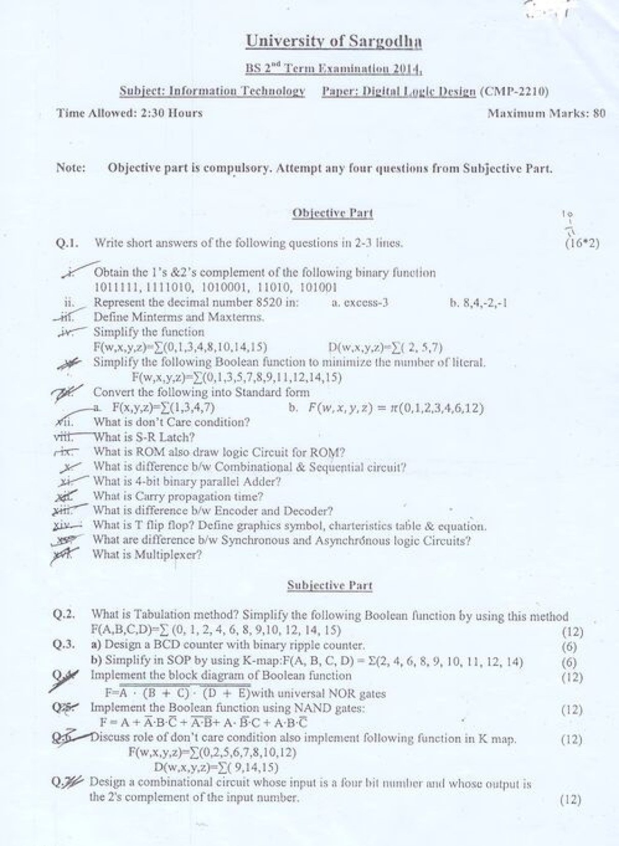
Digital Logic Design BS IT 2nd Term Past paper 2014 UOS

University of Sargodha
BS 2nd Term Examination 2014
Subject: Information Technology
Paper: Digital Logic Design (CMP-2210)
Time Allowed: 2:30 Hours
Maximum Marks: 80
Objective Part
Q.1. Write short answers of the following questions in 2-3 lines.
- Obtain the 1’s & 2’s complement of the following binary function
1011111, 1111010, 1010001, 11010, 101001 - Represent the decimal number 8520 in:
a. excess-3
b. 8.4, -2, -1 - Define Minterms and Maxterms.
- Simplify the function
F(w,x,y,z) = Σ(0,1,3,4,8,10,14,15)
D(w,x,y,z) = Σ(2, 5, 7) - Simplify the following Boolean function to minimize the number of literal.
F(w,x,y,z) = Σ(0,1,3,5,7,8,9,11,12,14,15) - Convert the following into Standard form
a. F(x,y,z) = Σ(1,3,4,7)
b. F(w,x,y,z) = π(0,1,2,3,4,6,12) - What is don’t Care condition?
- What is S-R Latch?
- What is ROM also draw logic Circuit for ROM?
- What is difference b/w Combinational & Sequential circuit?
- What is 4-bit binary parallel Adder?
- What is Carry propagation time?
- What is difference b/w Encoder and Decoder?
- What is T flip flop? Define graphics symbol, characteristics table & equation.
- What are difference b/w Synchronous and Asynchronous logic Circuits?
- What is Multiplexer?
Subjective Part
Q.2. What is Tabulation method? Simplify the following Boolean function by using this method
F(A,B,C,D) = Σ(0, 1, 2, 4, 6, 8, 9, 10, 12, 14, 15) (12)
Q.3.
a) Design a BCD counter with binary ripple counter. (6)
b) Simplify in SOP by using K-map: F(A, B, C, D) = Σ(2, 4, 6, 8, 9, 10, 11, 12, 14)
Implement the block diagram of Boolean function (12)
Q.4. Implement the Boolean function using NAND gates:
F = A + A’BC + AB + A’BC + A.B’C (12)
Q.5. Discuss role of don’t care condition also implement following function in K map.
F(w,x,y,z) = Σ(0,2,5,6,7,8,10,12)
D(w,x,y,z) = Σ(9,14,15)
Q.6. Design a combinational circuit whose input is a four bit number and whose output is the 2’s complement of the input number. (12)
